We want to keep you in the loop! Our website is currently undergoing some exciting enhancements to provide you with an even better online experience.
Digital Control of Medium-high Power DC-DC Converters (Full version)
24-hour online training – Time zone: CET
Dates
July5th – 6th – 7th and 19th – 20th – 21st, 2021
Training duration
6 days, 4 hours per day
Course fees
For Part 1 & 2:
1 600 Euros* per person (Exc VAT) for industrial participants.
900 Euros* per person (Exc VAT) for academic participants. * (A 3% fee is applied for credit card payments). Payment will be due before the training.
Fees include 6-day training and training materials.
For Part 1, 2 & 3:
2 400 Euros* per person (Exc VAT) for industrial participants.
1 200 Euros* per person (Exc VAT) for academic participants. * (A 3% fee is applied for credit card payments). Payment will be due before the training.
Fees include 6-day training and training materials.
EARLY BIRD (till June 11th, 2021)
Benefit from 25% of discount on the course fees if you register before June 11, 2021:
1 800 Euros* per person (Exc VAT) for industrial participants.
900 Euros* per person (Exc VAT) for academic participants. * (A 3% fee is applied for credit card payments). Payment will be due before the training.
Registration deadline
The registration will be closed by June 28, 2021.
Number of seats
No more seats available for Part 3 but you can still register for Part 1 & 2.
The main objective of the training is to provide the audience with the technical competence to design the digital control of power converters.
In this case, the medium-high power DC-DC converters have been used as a case study to show the digital control techniques. However the concepts can be used, directly, in other applications such as DC-AC inverters or AC-DC PFC.
In addition to the theoretical concepts on converter topologies, dynamic modeling and analysis of the specific effects of the digital loop, the course aims to be practical and allow the participant to “learn by doing”.
In the practical sessions, the participant must program in Code C the complete control loop from the scratch. In the additional practical sessions, the student will be able to program a digital HW board based on a System on Chip device (microprocessor + FPGA) and perform different experiments with which to assess the performance of the control developed.
What should you expect from the training?
This course is an introductory to advance-level course focused in the following specific objectives:
To review the main DC-DC converter topologies for medium-high power applications. Unidirectional and Bidirectional converters with and without galvanic isolation are covered: Multiphase Synchronous- Buck Converter, Phase-sifted Full-bridge converter, Dual Active Bridge, LLC and CLLC resonant converters, Four Switches Buck-Boost Converter.
The steady-state operation is described in detail together with the main design aspects.
Dynamic modeling and control reference designs are provided. Ready-to use simulation examples are included for all the case studies.
To study in depth the main concepts of digital control:
Gain and resolution of DPWM as well as practical implementation examples.
Sampling techniques and digital delay.
Analog and digital current and voltage filtering.
Gain and resolution of ADC resolution.
Compensator design and constants resolution.
Limiters and anti-windup function.
Unity gain feedback.
Limit cycles, Etc.
To show an efficient methodology based on programming the control through C blocks in PSIM and generating automatic code for the FPGA through the HLS module. Finally, to integrate the control performed in the FPGA with the functions performed with the microprocessors.
To show some practical techniques such as the measurement of frequency response when the modulator is digital and the measurement of internal signals from the FPGA and/or microprocessors by ADC.
Audience description
This training course is recommended to everybody interested in the theoretical and practical design aspects of medium-high power converters and its control by means of digital control techniques. On the other hand, the course is eminently practical, therefore, the complete implementation of the control loop will be shown and experimentally verified.
All the audience will find a set of practices to develop, from the scratch, a digital control of a power converter using SoC devices.
The practicing engineer (firmware and power hardware engineers) will be given with the physical meaning and efficient explanations of the modeling and digital control problem.
The university student (Master and PhD degrees) will find easy-to-follow mathematical developments not always covered in the textbooks.
Instructors and university professors will find a different approach for their explanations as well as an interesting set of simulation reference designs.
The digital control expert is also invited to participate in a discussion-space to share practical experiences on specific problems.
Course structure
The Full Version Course is structured in the following blocks:
Part 1
Theoretical contents, simulation and design examples
3 days
Part 2
Online practice: design and simulation case studies
1 day
Part 3
Online practice: FPGA Programing and experimental test
2 days
Part 3 is opened only to participants who will have participated to Part 1 & 2 either at the reduced version course on March 8, 11, 15 and 18 or the full version course on July 5, 6, 7, 19 and 20.
Note: every day of the course, the session will be of 4 hours.
Price structure
When registering to the Full Version Course, you will be offered three options:
Session 1: registration for part 1 & 2 with following pricing:
1 600 Euros* per person (Exc VAT) for industrial participants
900 Euros* per person (Exc VAT) for academic participants
Session 2: registration for part 3 only (condition: part 1 & 2 has to be done) with following pricing:
800 Euros* per person (Exc VAT) for industrial participants
300 Euros* per person (Exc VAT) for academic participants
Session 3: full registration with following pricing:
2 400 Euros* per person (Exc VAT) for industrial participants
1 200 Euros* per person (Exc VAT) for academic participants
* (A 3% fee is applied for credit card payments). Payment will be due before the training.
Methodology
The focus is placed on Concepts
The explanations are focused on the concepts and physical meaning. Mathematical developments are also included as reference materials in annexes.
Tools
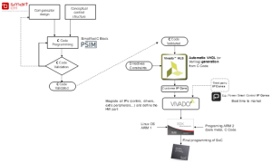
The methodology is summarized in Fig. 1. The steps are the following:
Step 1: Develop the Controller design using SmartCtrl.
Step 2: Use PSIM functional blocks to have a first conceptual control scheme.
Step 3: Use PSIM C Block to develop the complete control structure for the digital control implementation.
Step 4: Simulate the power stage and the control structure contained in the C Block to validate the control C code. Note that this code is quite similar to the final microprocessor code and FPGA code.
Step 5: Use Vivado HLS to automatically generate VHDL code from the already validated C code.
Step 6: Experimental test using the PSC Hardware Experimental Kit.
In these steps, the participant performs a “learn by doing” process. At the end of the training the participant has developed a complete digital control in a SoC.
Examples & Exercises
A large number of examples are used to show training explanations. A large number of “ready to use” C Code for the main loop blocks will be also provided (DPWM modulator, PID compensators, etc.) Exercises are proposed to be developed before the Practice Sessions. Then they will be resolved during the training.
Fig. 1: Control Design & Programing Flowchart
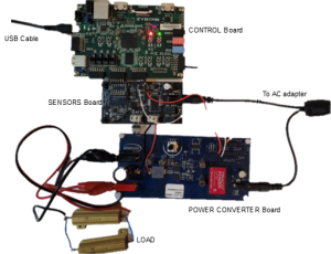
Online hardware practices (part 3) will be developed using the Hardware Experimental Kit shown in Fig. 2. Power Smart Control S.L. (PSC) will provide each participant with a HW Experimental Kit that will be returned upon completion of the course. A deposit of 500€ will be asked.
Fig. 2: PSC HW Experimental Kit
Instructor
Dr. Antonio Lázaro, Professor at Carlos III University of Madrid and Technical Director at Power Smart Control S.L.
Antonio Lázaro was born in Madrid, Spain, in 1968. He received the M. Sc. in electrical engineering from the Universidad Politécnica de Madrid, Spain, in 1995. He received the Ph. D. in Electrical Engineering from the Universidad Carlos III de Madrid in 2003.
He has been an Assistant Professor of the Universidad Carlos III de Madrid since 1995. He has been involved in power electronics since 1994, participating in more than 80 research and development projects for industry. He holds 10 patents and software registrations and he has published nearly 140 papers in IEEE journals & conferences. His research interests are high-power DC-DC Converters, Power Factor Correction (PFC) Rectifiers, AC-DC inverters (railway and grid-connected applications), modeling and control of switching converters and digital control techniques.
Dr. Lazaro has originated and leaded the development of the Software SmartCtrl. He is the co-founder and technical director of Power Smart Control S.L. a spin-off company of Carlos III University of Madrid focused on the development of SmartCtrl and hardware high added-value control solutions for power electronics (SoC-FPGA control, HIL systems, real-time FPGA variable logging, automatic test-benches, etc.).
Language
English
Computer and temporary PSIM and SmartCtrl licenses
Each participant will have to bring a personal computer.
PSIM and SmartCtrl temporary licenses will be provided for the duration of the course.
Hardware Experimental KIT
Power Smart Control S.L. (PSC) will provide each participant with a HW Experimental Kit that will be returned upon completion of the course. A deposit will be asked..
Program:
Day 1- July 5, 2021 | ONLINE THEORETICAL SESSION
9 am – 11 am (2 hours) | Section I- Non-isolated and isolated topologies revision and steady-state analysis
Options to represent the digital loop: SSS / SSZ / ZZZ
Discretion of small-signal modles
Discrete modeling techniques
Day 2 – July 6, 2021 | ONLINE THEORETICAL SESSION
9.30 am – 11 am (2 hours) | Section III: Modeling examples & control reference design
Multi-phase synchronous buck converter (MSB)
Phase-shift full bridge (PSFB)
Input series – Output parallel modular converters
Input parallel – Output series modular converters
11 am – 11.15 am: Coffee break
11.30 am – 1.15 pm (2 hours) | Section III: Modeling examples & control reference design
Single-phase dual active bridge (DAB)
LLC converter
Four switches Buck-Boost converter
Day 3 – July 7, 2021 | ONLINE THEORETICAL SESSION
9 am – 11 am (2 hours) | Section IV: Digital PWM modulator and sampling techniques
Modular block
Digital sawtooth carrier waveform
Digital triangular carier waveform
PWM Modulator
Resolution and gain of PWM modulator
Dead-times
Analog voltage and current sensors
Hall effect current sensors
Single ended and differential analog amplifiers (transmitters and receptors)
Isolated voltage amplifiers
Sampling techniques
Introduction
Sampling techniques of output voltage
Analog and digital filters
Sampling techniques of inductor current. Triangular and Sawtooth carrier waveforms
ADC Management: clock and SPI
ADC Resolution and ADC gain
Sensor and ADC gains rescaling looking for unity gain feedback
11 am – 11.15 am: Coffee break
11.15 am – 1.15 pm (2 hours) | Section V: Digital delay & Compensator Design and Implementation
Digital delay
Physical concept
Transport delay and PWM delay
Effect on the loop transfer function
Single and double update
Multisampling techniques
Effect on feedforward compensations
Sampling and modulating signal update scenarios
Single update and double update PWM
Multi-sampling techniques
Sampling techniques of inductor current. Triangular and Sawtooth carrier waveforms
Oversampling and moving average filter
Digital compensators
Digital PI and PID
Transfer functions and difference equation
Anti-windup
Day 4 – July 19, 2021 | ONLINE PRACTICE – SIMULATION
Notes for on-line practice:
The wording of Exercises 1 -7 is sent in advance to the audience. The objective is the participants tries to solve previously the exercised and then use Day 4 session to solve doubts and finishing the exercises.
Complete solution of Exercises 1-7 is given to the participants: slides and design and simulation files.
9.00 pm – 11.00 pm (2 hours) | Section VI: Simulation of a complete digital control loop
Exercise 1: PSIM C-block Implementation of a complete digital control for Boost Converter
Power stage. PSIM components
DPWM. PSIM C-block Implementation
Digital delay emulation. PSIM C-block Implementation
ADC. PSIM C-block Implementation
Analog voltage sensor: Gain, offset & bandwidth. PSIM components
Elements to get unity feedback gain. PSIM components
Exercise 2: Basic Simulation in open loop to check the correct operation of the different blocks
Exercise 3: AC sweep simulation of loop transfer functions
Modulating signal to output voltage transfer function, G1(jω)
Output voltage to feedback voltage transfer function, G2(jω). Check if unity gain is obtained. Obtain a simplified model for the complete sensing network
Exercise 4: Design and implementation of PID compensator. using
Use Kp, Ti and Td as input parameters
Parallel implementation must be considered
Design the compensator to stabilize the transfer function G1(jω) x G2(jω), using SmartCtrl equation editor for the compensator block.PSIM C block implementation of PID compensator with anti-windup function
11 am – 11.15 am: Coffee break
11.15 am – 1.15 pm (2 hours) | Section VI: Simulation of a complete digital control loop
Exercise 5: PSIM simulation of the complete circuit under step changes on input voltage and load current
Additional exercises
Exercise 6: Developing a complete theoretical model using SmartCtrl Equation Editor for the following blocks:
Digital PWM modulator + digital delay + boost power converter. Compare the frequency response in SmartCtrl against the simulated AC sweep of G1(jω)
Voltage sensor, analog signal conditioning, ADC, unity-gain-feedback block. Compare the frequency response in SmartCtrl against the simulated AC sweep of G2(jω)
Exercise 7: Limit Cycles. Reduce the resolution of the DWPM to be below the bits number of the ADC. Simulate the closed loop operation of the converter.
SmartCtrl-PSIM C Block-HLS Methodology
How to Download And Install Xilinx Vivado Design Suite
Day 5 – July 20, 2021 | ONLINE HARDWARE PRACTICE
Notes for on-line practice:
Practice 1 will be a guided practice and some VHDL IP cores will be given in advance to the audience.
The wording of Practice 1 – 2 is also sent in advance to the audience. The objective is the participants tries to solve previously the practice and then use Day 5 session to solve doubts and finishing the exercises.
Complete solution of Practice 1 – 2 is given to the participants: slides, design and simulation files, and microprocessor and FPGA programing files.
9.00 pm – 11.00 pm (2 hours) | Practice 1: Control Blocks Generation in Vivado
Basic description of Vivado Design Suit
How to create a new project
Loading the Board files in the Zybo board
Basic code structure
General operation of an IP core
HLS / VHDL blocks generation
DPWM modulator in VHDL / HLS
HLS PID compensator including anti windup and feed-forward compensations
VHDL ADC driver
Synthetizing a new system in the SoC device
RTL exportation to Vivado
Project creation
Zynq configuration
Generation of the IP manager block
Exporting the hardware description to SDK
11 am – 11.15 am: Coffee break
11.15 am – 1.15 pm (2 hours) | Practice 2: AC Sweep Test in digital domain
A first HW experiment
Zybo board and power board connection
Basic Console to parameterize e.g. duty cycle
Testing the open loop operation
Modulator structure
Duty cycle perturbation
Delays subtraction
Measurement of the open loop gain Gvd
Measurement of the open loop Gid
Day 6 – July 21, 2021 | ONLINE PRACTICE
9.00 pm – 11.00 pm (2 hours) | Practice 3: Voltage Mode Test
Synthesis of a new project including the current ADC driver
Generation of the current ADC driver block
Generation of the variable voltage reference block
Basic Closed loop operation
Synthetizing a new project including the ADC driver
Testing the effect of PID constants
Testing the effect of the anti-windup
11 am – 11.15 am: Coffee break
11.15 am – 1.15 pm (2 hours) | Practice 4: Current Mode Test
Synthesis of a new project including the current ADC driver
Generation of the current ADC driver block
Generation of the variable current reference block
Please register as early as possible if you plan to attend the training. As soon as the minimum of participants is reached, POWERSYS will confirm the course.
The registration to the course includes the lunches and coffee breaks. Participants will have to pay 100% in advance before the course.
Cancellation can be made according to POWERSYS’ General Conditions for courses:
Withdrawal from the Course:
In case you cannot attend the course after having registred, please contact us as soon as possible at marketing@powersys.fr
In case of cancellation three weeks OR MORE before the beginning of the course, the participants will not be charged.
In case of cancellation less than three weeks before the beginning of the course, POWERSYS will charge the participant 50% of the course fees.
Please note that POWERSYS will not reimburse any travel and/or accommodation expenditure in case of cancellation of the course. We recommend you to make your travel arrangements once the course is confirmed.
For French participants:
POWERSYS est enregistré en tant que prestataire de formation (auprès du Préfet de la Région Provence-Alpes-Côte d’Azur sous le numéro 93 13 13256 13). Une convention de formation peut être établie sur demande avant la date de formation.
As part of our rebranding efforts, Powersys is updating this website to better communicate and engage with our valued clients. To provide the best possible support, we’re revamping the user interface, a project that will take place through early 2023.
In the meantime, you may access the existing version here.
If you have questions or concerns, please contact marketing@powersys.fr
Our website uses cookies for statistical purpose to improve user experience and provide relevant content. If you continue browsing without changing your settings, you consent to our use of cookies. More information can be found in our Privacy Policy. OkPrivacy policy